tenstorrent blackhole architecture guide
deep dive into the tenstorrent blackhole p100a architecture — tensix cores, NOC routing, firmware stack, and the open-source toolchain.
I bought a Tenstorrent blackhole p100a. The idea of a fully open source toolchain, from the kernel mode driver to the software stack that runs the models, is super exciting. Some parts of the card (like the firmware binaries for certain tiny components) aren’t open source because of 3rd party IP, but this is pretty much the best it gets. You own every part of the card above the Verilog.
The hardware also has potential. Since they haven’t raised prices yet (as of 2/28/26), you can get a card with 28GB GDDR6 (yes, it’s slow; it’s the main bottleneck) that has approximately equal matmul performance to a 5090 for $999! And there’s a “buy now” button on the website!!
Additionally, there is a $2,000 bounty on getting blackhole supported in tinygrad ($1k from tinygrad and $1k from Corsix on Twitter).
Update: the tinygrad bounty has actually disappeared following this tweet from tinygrad.
Repos referenced in this project, from the lowest to highest level
- Firmware images and flashing tool —
tt-firmware / tt-flash - Card firmware:
tt-zephyr-platforms - Hardware debug tooling (bring-up / deep debug) —
tt-exalens / luwen - ISA documentation (low-level correctness reference) —
tt-isa-documentation - Kernel-mode driver (Linux device access plumbing) —
tt-kmd - User-mode driver (host API layer above KMD) —
tt-umd - Tensix SFPI toolchain bits (kernel toolchain ecosystem) —
sfpi - Low-level kernels (LLK building blocks + dataflow) —
tt-llk - Runtime + kernel authoring entrypoint (TT-Metalium + TTNN examples) —
tt-metal - Any abstractions above this are impossible to keep track of and reason about, so I haven’t even bothered to read any code outside of these repos.
This article serves as a reference to the low level workings of the Blackhole p100a (and p150b, by extension, as most of the same concepts apply) and as a guide to anyone who wants to understand how these cards work and perhaps help write the tinygrad backend for it. At the moment, the runtime and low level firmware is finished (blackhole-py is capable of executing any tt-metal kernel using pure Python, no dependencies). You still need to have the tt-metal risc-v compiler toolchain downloaded, but instead of making the user build tt-metal from source, I just package a tarball containing only the required headers and binaries.
device firmware and startup
You don’t need to know anything about the device firmware to figure out how the card works (we’re only touching above this layer). The only reason this section is included is because I spent 5 or 6 hours in Ghidra trying to decompile the firmware bundle in tt-firmware to search for the fan control logic. This card has a single-fan blower style cooler, and by default the fan curve is set very high (40% when the temp is under 49c). Shortly afterwards, I realized tt-zephyr-platforms (their firmware) was open source. I made a quick change, flashed the new firmware, and then the noise was gone! You can also change the fan speed dynamically by sending a message to the ARC tile: this is a short python script to do that.
hardware / programming model: Everything is tile.
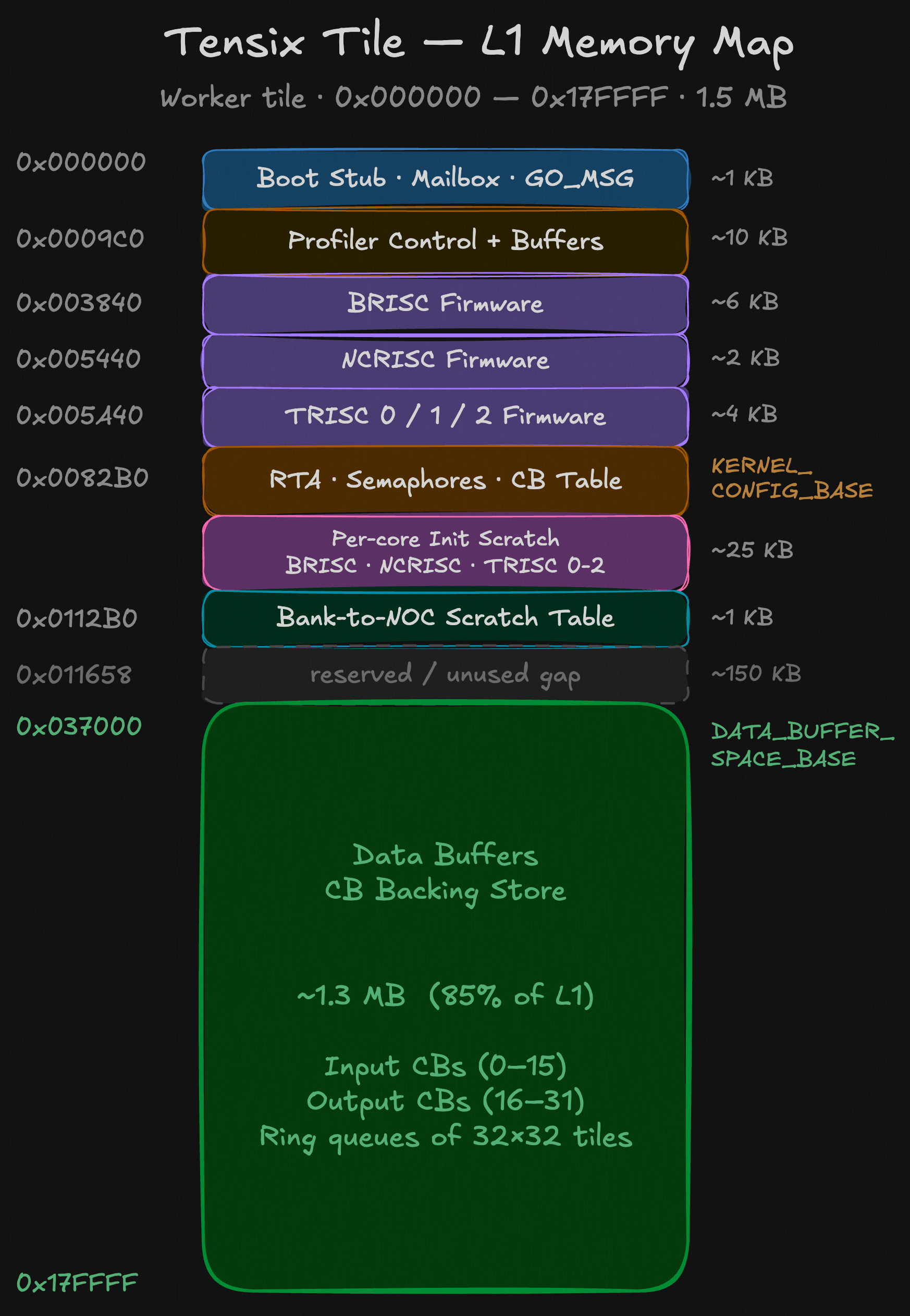
Each Tensix tile packs 1.5 MB of L1 SRAM (input/output circular buffers plus kernel, scratch and semaphore space), five RISC-V cores — ncrisc reads, the three trisc cores unpack → math → pack, and brisc writes — and the Tensix coprocessor: a matrix engine fed by double-buffered srcA/srcB banks and an SFPU for transcendentals, both writing into the shared Dst register.
This is the tile diagram / layout for the p150b (the full non-binned card). All tiles in this grid can communicate with each other via 2 NoCs (networks on chip). Communication to host is routed through the PCIe tile (PCIe 0 on p100a and PCIe 1 on p150b).
harvesting (p100a) The tile layout on the p100a has the rightmost 2 columns of Tensix tiles and 1 bank (4GB) of dram fused off, but the exact coordinates of the disabled tiles vary from board to board. On my p100a, DRAM bank 3 is fused off.
NoC
This layer serves as the communication fabric connecting every Tensix tile. It consists of two Networks-on-Chip (NoCs) that operate in opposite directions.
The first network, noc0, originates at the top-left corner of the grid, and packets on this network can only move downward or to the right. The second network, noc1, originates at the bottom-right corner, and packets on this network can only move upward or to the left.
Both networks can be used concurrently. In typical usage, noc0 is used to read data from DRAM, while noc1 is used to write data back to DRAM. Separating reads and writes onto different NoCs avoids head-of-line blocking that would otherwise occur if read and write traffic shared the same unidirectional ring.
It wraps around; if you wanted to send a message from T121 to T0, it would wrap around the right edge and end up at the top left.
noc0 routes right → down from the top-left; noc1 routes left → up from the bottom-right.
DRAM ports (columns 0 & 9) l2cpu / PCIe / ARC / eth — ignored by multicast
click a tile to move the destination · shift-click to move the source
Tiles can be accessed by their coordinate (x,y). On the p150b (the full card) there are 17 columns and 12 rows. On p100a, there are 14 columns.
Each NoC has two modes for writing data: unicast and multicast. Multicast is a massive speedup when you have to issue the same writes to many tiles (uploading firmware, kernel binaries, etc). Due to the number of Tensix tiles, you’ll lose considerable performance if you try to unicast write to every single core sequentially, so multicasts are imperative. A multicast is addressed with a rectangle of tiles (a start and end NoC coordinate); the packet routes to the box’s entry corner and then fans out to every tile inside it. Flip the routing widget above to multicast and drag a box to watch the packet fan out.
On the host, you can access tile memory by using the allocate_tlb ioctl to open a 2MB TLB window and then configuring it with a base address offset and two NoC coordinates (start, end) with the configure_tlb ioctl. You can also set mcast=True here. This returns two mmap offsets into the PCIe bar (UC, WC); all reads and writes here get translated into NoC reads and writes by the PCIe tile. This is the core mechanism behind the TT_USB=1 slow dispatch mode in blackhole-py. This gives you access to the L1 memory in each tile, all the registers, the RAM used by each core in the Tensix tile, etc. This is enough to launch kernels and run workloads on the card.
It’s called TT_USB in
blackhole-pybecause this is the only way you can use the card if you have it connected via a UT3G USB4 adapter. More info on this later.
arc tile (1)
This tile reports fan speed, harvesting and telemetry information, and clock speed / power usage. It’s the system management tile.
dram tiles (D)
These aren’t really “tiles”, they’re more like ports into the GDDR6 controllers. On the p100a, there are 7 GDDR controllers, each backing a 4GB memory bank, for a total of 28 GB. Each controller is exposed through a group of three DRAM tiles (for example, all D0 tiles point to the 0th controller).
The DRAM allocator is quite simple. A tensor is split into seven equal parts (one per 4GB bank), and tiles are distributed uniformly. The API makes this straightforward.
const InterleavedAddrGenFast<true> dram = {
	.bank_base_address = dram_addr,
	.page_size = page_size,
	.data_format = DataFormat::Float16_b, // bfloat16
};
There are two ways to access DRAM:
- Perform a WC
mmapwrite directly to the PCIe BAR exposed through a TLB window on a DRAM tile. - Launch a dataflow kernel on the brisc or ncrisc cores that performs
noc_async_read_tile/noc_async_write_tile.
p100a dram bandwidth benchmark (512 MB xfer)
| Direction | 1. Raw MMIO (slow) | 2. Fill/Drain Kernels (fast) | Speedup |
|---|---|---|---|
| Host → DRAM (write) | 3.93 GB/s | 29.51 GB/s | 7.5x |
| DRAM → Host (read) | 0.032 GB/s | 45.78 GB/s | 1438x |
The MMIO read path is catastrophically slow (~32 MB/s) — that’s the uncacheable PCIe BAR read penalty. Kernel-based reads bypass that entirely by having the Tensix cores DMA data into pinned sysmem, hitting ~46 GB/s.
Writes are less dramatic but still a solid 7.5x improvement with kernels, since MMIO posted writes (~3.9 GB/s) are already reasonably fast through the write-combining TLB path.
One architectural detail that’s hard to justify is the presence of three DRAM tiles per bank. In practice, tt-metal selects a single tile from each three-tile group (e.g., D0, D3, D6, …) and uses only that one as the access point for the bank. The other two tiles in each group remain unused.
Round-robin scheduling across the three tiles within a bank would not increase effective bandwidth, since all three ultimately feed the same GDDR controller. From a software perspective, they behave as redundant front-ends to a single memory endpoint rather than independent channels.
l2cpu (16)—SiFive x280
These are wasted silicon. I see absolutely no use for these. The cores are too slow to be used for anything serious, and while you can run Linux on them, it’s not a particularly fun experience. It is possible to address the other Tiles from these cores, but it will be slow and therefore not practical. The SiFive X280 is a high-performance in-order RISC-V core, so the choice of CPU isn’t the problem — it’s the bandwidth and latency of going through the NoC to reach DRAM that makes it impractical for anything real.
ethernet (E)
These are all disabled on p100a, so I haven’t been able to experiment with them. They’re mainly used for distributed training, i.e. multiple tenstorrent cards in the same system would communicate over ethernet instead of through the host (PCIe).
pcie
There are two PCIe tiles in the grid, but only one is ever active. On the p100a, PCIe tile 0 is enabled and tile 1 is disabled; on the P150b, it’s the reverse.
Functionally, a single PCIe tile handles all host communication. It translates MMIO writes (via TLB windows mapped into the PCIe BAR) into NoC transactions and manages general PCIe traffic. There’s no mode where both tiles are active or where bandwidth is shared between them.
Given that one tile is sufficient, it’s unclear why the design includes two instead of having both SKUs use the same one. The second tile seems to exist for layout, binning, or SKU flexibility rather than for concurrent use.
tensix (T)

These tiles are responsible for all AI compute. Inside each Tensix tile there are 5 baby RISC-V cores, a Tensix coprocessor, and 1.5 MB of L1 memory. It’s called L1 because of the memory speed; it’s not cache. There is no cache anywhere on this card.
A kernel executes similarly to how it would on a GPU, but with notable differences in how the computation is actually done.
Write tensors to global DRAM.
ncrisc: Reads from global memory, pushes a tile into the CB (circular buffer).
trisc0: Unpacks tile and copies to the Tensix coprocessor’s registers (SFPU).
trisc1: Sends compute ops to the compute engine (tensix coprocessor). This is where the compute happens.
trisc2: Packs tile and copies from the compute engine’s dst register into the output CB.
brisc: Writes tiles from output CB back to global memory.
Note: The roles of ncrisc and brisc are commonly interchanged in tt-metal, you can switch them and your program will function the exact same.
A circular buffer is just a ring queue of tiles stored in the L1 memory of each tile. Each tile has 32 CBs; the first 16 are input, and the last 16 are output. For example, if you were adding two tensors, you would need 3 CBs: Tensor A (CB 0), Tensor B (1), and then the output Tensor (16).
The tile abstraction goes one level deeper. Each entry in a circular buffer is a 32×32 matrix in some datatype, physically organized as four 16×16 “faces.” The circular buffer itself is just a ring of these tiles in L1, and you can choose how many tiles it holds, bounded only by the ~1.5 MB of L1 available per tile (minus kernel code and scratch space).The kernel binary, scratchpad, and per-core RAM eat into L1, so in reality you have a bit less — around 1.3 MB — usable for CBs. The four-face layout is a hardware constraint from the FPU’s internal register organization, not an arbitrary software choice — the unpacker has to feed data into the FPU in 16×16 chunks.
Because the hardware operates strictly on 32×32 tiles, tensors that don’t naturally align to that shape must be padded before upload. The compute kernel then has to account for the padded regions so that zeroed elements don’t affect the result. The unpack and pack stages exist to bridge this mismatch: they translate between the flat tensor layout in DRAM/L1 and the internal data layout expected by the Tensix coprocessor, which follows a different tilized representation.
The main point of the CB is that you can overlap reading/writing to/from DRAM with compute. Your compute tile can consume tiles from the CB when they’re marked as ready while more tiles are being read from DRAM. Same for writing.
tensix coprocessor
This is a fully custom coprocessor built by Tenstorrent. The trisc1 core does not actually run the compute — it’s just responsible for dispatching ops to this coprocessor. If you disassemble the trisc1 ELF and read the raw rv32 instructions, you’ll see some that start with tt; these are custom additions to rv32 that dispatch a particular op to the coprocessor. The instruction set and behavior is mostly documented in tt-isa-documentation.
There are two computation paths: the SFPU and the Matrix engine. They ultimately write to the same destination register, dst, which can be viewed two ways depending on the output datatype.
| Buffer | Logical shape | Capacity | Typical use |
|---|---|---|---|
| dst16b | 1024 rows × 16 cols × 16b | 16 tiles (8 per half) | bfloat16/float16 accumulation |
| dst32b | 512 rows × 16 cols × 32b | 8 tiles (4 per half) | fp32 accumulation |
In 32-bit mode, each logical row spans two physical rows (high 16b in row R, low 16b in row R+8), so same physical storage, half the logical rows.
matrix engine / fpu
The FPU uses 4 registers, 2 srcA and 2 srcB. Both are 64 rows by 16 cols, 19 bits per entry. The entries are 19 bits wide to accommodate tf32 inputs. In 16-bit datatypes, the low 3 mantissa bits are zeroed. Interestingly, the bits are stored in a shuffled layout: {Sign, Mantissa, Exponent}, not the typical IEEE order.
The two banks per register enable double-buffering: at any moment, one bank is owned by the Unpackers (being filled from L1), the other by the Matrix Unit (being read for compute). The flip happens as part of the compute instruction itself — every MVMUL, ELWMUL, etc. has FlipSrcA and FlipSrcB bits. When set, the instruction releases its current bank back to the unpackers and switches the FPU’s bank pointer to the other bank:
if (FlipSrcA) {
	SrcA[MatrixUnit.SrcABank].AllowedClient = Unpackers;
	MatrixUnit.SrcABank ^= 1;
}
If the FPU tries to read from a bank that the unpackers haven’t finished writing yet, the instruction stalls at the Wait Gate until ownership is transferred. The unpackers do the reverse — when they finish filling a bank, they hand it to the Matrix Unit and flip to the other bank. This way the unpackers can be filling the next set of operands while the FPU is computing on the current set, hiding the unpack latency.
| instruction | operation | throughput @ 1Ghz (1 tile) |
|---|---|---|
| MVMUL | dst += srcB @ srcA (matmul) (lowest precision) | 4.096 tflops |
| ELWMUL | dst = srcA * srcB (element-wise) | 0.256 tflops |
| ELWADD | dst = srcA + srcB | 0.128-0.256 tflops (with AddDst) |
| ELWSUB | dst = srcA - srcB | 0.128-0.256 tflops (with AddDst) |
| GMPOOL | dst = max(dst, max_along_cols(srcA)) | 2.048 tflop/s |
| data movement operations | ||
| MOVA2D | move 1 row or all 16 cols from srcA’s current bank to dst. also does format conversion | |
| MOVB2D | like MOVA2D (reads from srcB) and has broadcast modes: 1 row, 4 aligned rows, 1 src row -> 8 dst rows, col 0 replicated to all 16 columns | |
| MOVD2A | 1 or 4 aligned rows from dst to srcA. can apply inverse format conversion. you must wait (STALLWAIT) manually. 2-cycle latency | |
| MOVD2B | Like MOVD2A, but writes to srcB. 3-cycle latency. for the next 3 cycles, only another MOVB2B instruction can be issued | |
| MOVB2A | srcB -> srcA. direct 1 or 4 row copy, no format conversion. auto waits on srcB but not on srcA. 4-cycle latency | |
| ZEROACC | does not write zeros. clears DstRowValid bits so subsequent readers interpret those rows as the identity element (0 for add/mul, −∞ for max-pool). modes: clear 1 row, 16 rows, 512 rows (half), or all 1024. 1-cycle latency | |
| ZEROSRC | actually writes all 64 x 16 elements of the target bank. NegativeInfSrcA=1 writes all-ones (−∞) to srcA for max-pool init. can target one bank or both. | |
| SHIFTXA | shift 16 srcA rows by 1 column. the vacated lane is zero-filled. | |
| SHIFTXB | shifts a single configurable row of srcB left by 1 column. ShiftInZero=0 rotates cyclically; ShiftInZero=1 zero-fills. 2-cycle latency, 1-cycle dead after each. | |
| TRNSPSRCB | In-place matrix transpose of SrcB rows 16-31. Hardwired. 1-cycle latency. |
The AddDst flag on ELWADD and ELWSUB gives you dst += srcA + srcB at 2x the throughput of the non-accumulating version.
GMPOOL also supports ArgMax=true for getting the index of the max element.
The FPU multiplier consumes 5 bits of srcA mantissa + 7 bits of srcB mantissa per phase. More phases adds precision but reduces the speed of computation. LoFi is the lowest precision (1x throughput), and it halves every step (HiFi2 and HiFi4). The eltwise and gmpool ops are not affected by this precision setting.
matmul precisions There are a few different precision options for matmuls: each mode consumes more mantissa bits than the last. The matmul engine runs in steps, multiple fidelity phases process different slices of the mantissa and accumulate the partial products.
LoFi: 1 multiplier step. Reads 5 mantissa bits from srcA and 7 mantissa bits from srcB.
HiFi2: 2 multiplier steps. Reads next 5/7 bits.
HiFi4: 4 multiplier steps.
Each phase just replays the same MVMUL instructions again, with a register configured to tell the processor which fidelity phase it’s on. LoFi takes 16 MVMUL instructions per tile and HiFi4 takes 64, hence the 4x throughput decrease. Generally, for 16-bit inputs, HiFi2 is enough precision. You only need to use HiFi4 if your inputs are tf32.
sfpu
The SFPU handles transcendentals and other misc ops not covered by the matrix engine. It operates on Lreg[17] (sfpu local registers) where each Lreg is 32 lanes, 32 bits per lane (sort of like an AMD wavefront). The 32 lanes are arranged as a 4x8 grid (4 rows of 8 lanes), which matters for SFPTRANSP (4x4 transpose within columns) and SFPSHFT2 (lane rotation). The SFPU does not read directly from CBs or L1. The data is read from Dst into Lreg, the operation is done, and then the result is stored back into Dst. Typically, the outputs of your computation will already be in Dst (imagine an FPU matmul just finished and you want to add on another op), or you can set trisc0 to unpack directly to Dst so that you can issue SFPU ops without having to use the matrix engine. The UNPACK_TO_DEST semaphore synchronizes trisc0 and trisc1 so SFPLOAD doesn’t read Dst before the unpacker finishes writing it.
Data movement instructions
| Instruction | Operation | Latency |
|---|---|---|
SFPLOAD | Dst → LReg (4 rows × 8 cols = 32 elements) | 1 cycle (load sub-unit) |
SFPSTORE | LReg → Dst (same 4×8 slice) | 1 cycle (store sub-unit) |
SFPLOADMACRO | Dst → LReg + schedule 4 pipelined ops across all 5 sub-units | 1 cycle |
SFPMOV | LReg → LReg copy, negate, or load config/PRNG | 1 cycle (simple sub-unit) |
SFPSWAP | Swap two LRegs (or min/max swap) | 1–2 cycles |
SFPTRANSP | 4×4 transpose within LReg[0:4] and LReg[4:8] lane groups | 1 cycle |
SFPSHFT2 | Lane rotation/shift (move data between SIMD lanes) | 1 cycle |
SFPLOADI | Load immediate constant → LReg (BF16, FP16, INT, etc.) | 1 cycle |
SFPCONFIG | Write LReg[0] lane 0 → constant register LReg[11–14] | 1 cycle |
SFPLoad format conversion
SFPLOAD also converts from Dst’s shuffled bit layout to proper F32 in Lreg:
| Mod0 | Reads Dst as | Produces in LReg |
|---|---|---|
FP16 | FP16 (5-bit exp) | FP32 (rebiased to 8-bit exp) |
BF16 | BF16 (8-bit exp) | FP32 (unshuffled) |
FP32 | FP32 (32-bit, 2 Dst rows) | FP32 (unshuffled) |
INT32 | Integer 32-bit | Sign-magnitude int32 |
INT8 | Integer 8 (±255) | Sign-magnitude int32 |
UINT16 | Integer 16 | Zero-extended uint32 |
SFPStore does the inverse conversion.
| index | access | contents |
|---|---|---|
| 0..7 | read/write | 8 general purpose, full fp32/int32 |
| 8 | read-only | 0.8373 (exp constant) |
| 9 | read-only | 0 |
| 10 | read-only | 1 |
| 11..14 | Programmable by SFPCONFIG | Constants: by default, Lreg[11]= -1.0 |
| 15 | read-only | Lane IDs: i = i * 2 |
| 16 | SFPLOADMACRO only | Macro pipeline scratch |
There are a lot of core instructions that are missing from the FPU op-set; for those, you have to include SFPU instructions. The SFPU is approximately 64x slower than the FPU, but you must use it for the following operations: This is the same fundamental tradeoff as Nvidia’s SFUs — transcendentals are expensive, and for most ML workloads the bottleneck is matmul anyway, so the throughput gap rarely matters in practice.
| Category | Operations |
|---|---|
| Division | div, recip (1/x) |
| Square root | sqrt, rsqrt |
| Exponentials | exp, exp2, expm1 |
| Logarithms | log, log2, log10, log1p |
| Trig | sin, cos, tan, asin, acos, atan, sinh, cosh, atanh, asinh, acosh |
| Activations | gelu, silu, sigmoid, tanh, elu, relu, leaky_relu, hardtanh, softplus, hardsigmoid |
| Error functions | erf, erfc, erfinv |
| Comparisons | <, >, <=, >=, ==, !=, where (ternary select) |
| Rounding | floor, ceil, round, trunc, frac |
| Bitwise | and, or, xor, not, left_shift, right_shift |
| Integer arithmetic | add_int32, mul_int32, div_int32, remainder, fmod |
| Type conversion | fp32↔fp16, fp32↔bf16, fp32↔int8, quantize/dequantize |
| Unary math | abs, neg, sign, square, power, clamp |
| Reductions (non-max) | cumsum, reduce_sum, Welford’s mean/variance |
| Special | dropout (PRNG), topk, polyval, fill |
MOP (micro-op processor) and the replay buffer
These are two separate hardware stages in the Tensix frontend pipeline that work together to keep the FPU fed at 1 instruction/cycle without the RISC-V core having to push every single instruction manually.
RISC-V core → MOP Expander → Replay Expander → Wait Gate → FPU/SFPU BackendTo matmul an entire 32x32 tile in 8x16 chunks (LoFi), you need to issue 16 MVMUL instructions. For a 4096x4096 matrix, this is 16,384 tiles * 16 = 262,144 MVMUL instructions. Without help, the RISC-V core would spend every cycle pushing instructions with no time for address setup, semaphore checks, etc. The MOP and replay buffer solve this by letting you fire off a single instruction that expands into thousands.
Replay buffer
The replay buffer is a 32-slot instruction buffer per thread. Each slot holds one 32-bit encoded Tensix instruction (not floats — these are uint32_ts storing TT instructions). You interact with it using the REPLAY instruction in two modes:
-
TT_REPLAY(index, count, exec=0, load=1)— record: captures the nextcountinstructions from the stream into the buffer starting atindex, without executing them. Setexec=1to also execute while recording. -
TT_REPLAY(index, count, exec=0, load=0)— playback: emitscountpreviously recorded instructions from the buffer starting atindex, at 1 instruction/cycle.
In software, the convention is that slots 0–15 are used for SFPU instruction sequences and slots 16–31 for FPU, but the hardware doesn’t enforce this — you can use all 32 for FPU if you have no SFPU instructions.
MOP expander
The MOP expander is a hardware loop controller that sits upstream of the replay buffer. You configure it via 9 write-only registers (MopCfg[0..8]), then issue a single TT_MOP(template, count, mask) instruction. The expander replaces that one instruction with a sequence of up to 32,639 instructions emitted at 1/cycle. While the MOP is expanding, the RISC-V core is free to do other work.
Because the MOP Expander sits before the Replay Expander in the pipeline, the MOP can emit REPLAY instructions as part of its expansion, and those get further expanded downstream into the recorded instruction sequences. The reverse is not possible — a replay expansion can’t contain MOP instructions.
There are two hardcoded templates. brisc cannot use MOP (its instructions enter the pipeline after the MOP Expander stage), but this doesn’t matter since brisc handles dataflow, not compute.
Template 0 (unpacker / mask template):
| Register | Name | Purpose |
|---|---|---|
| MopCfg[1] | Flags | bit 0 = HasB, bit 1 = HasA123 |
| MopCfg[2] | InsnB | instruction emitted when HasB (after A instructions) |
| MopCfg[3] | InsnA0 | main instruction per iteration |
| MopCfg[4] | InsnA1 | emitted after A0 if HasA123 |
| MopCfg[5] | InsnA2 | emitted after A1 if HasA123 |
| MopCfg[6] | InsnA3 | emitted after A2 if HasA123 |
| MopCfg[7] | SkipA0 | emitted instead of A0 when mask bit = 1 |
| MopCfg[8] | SkipB | emitted instead of InsnB when mask bit = 1 (if HasB) |
Called as TT_MOP_CFG(zmask_hi16) followed by TT_MOP(0, count-1, zmask_lo16). This roughly expands into:
for i in range(Count1 + 1):
    if mask_bit[i] == 0:       # normal face
        emit(InsnA0)
        if HasA123: emit(InsnA1, InsnA2, InsnA3)
        if HasB:    emit(InsnB)
    else:                       # skip face (zero-masked)
        emit(SkipA0)
        if HasB:    emit(SkipB)
This is how unpackers skip zero-faces in sparse tiles. The 32-bit zmask has one bit per face; 0 means unpack this face, 1 means skip it. trisc0 uses this to conditionally emit UNPACK vs NOP per face.
Template 1 (double-nested loop, used for matmul):
| Register | Name | Purpose |
|---|---|---|
| MopCfg[0] | OuterCount | 1–127 |
| MopCfg[1] | InnerCount | 1–127 (doubled automatically if LoopOp1 is not NOP) |
| MopCfg[2] | StartOp | emitted at top of each outer iteration (or NOP to skip) |
| MopCfg[3] | EndOp0 | emitted at end of each outer iteration (or NOP) |
| MopCfg[4] | EndOp1 | emitted after EndOp0 (or NOP) |
| MopCfg[5] | LoopOp | main inner loop body instruction |
| MopCfg[6] | LoopOp1 | if not NOP, alternates with LoopOp each iteration and InnerCount is doubled |
| MopCfg[7] | Loop0Last | replaces LoopOp on final inner iter of the final outer iteration |
| MopCfg[8] | Loop1Last | replaces LoopOp on final inner iter of a non-final outer iteration |
Which expands to:
for j in range(OuterCount):
    if StartOp != NOP:
        emit(StartOp)
    for i in range(InnerCount):
        if i < InnerCount - 1:
            emit(LoopOp)          # normal iteration
        elif j < OuterCount - 1:
            emit(Loop1Last)       # last inner iter, NOT last outer
        else:
            emit(Loop0Last)       # last inner iter OF last outer (the very end)
        # if LoopOp1 != NOP, swap LoopOp and LoopOp1 after each iteration
    if EndOp0 != NOP:
        emit(EndOp0)
    if EndOp1 != NOP:
        emit(EndOp1)
How they compose for matmul
For a single tile matmul, the LLK does:
-
Record 15 MVMUL instructions into the replay buffer (covering all but the last 8x16 sub-block of the 32x32 tile). These MVMULs use various addr_mods to step through SrcA/SrcB/Dst rows across the 4 faces.
-
Configure MOP template 1 with: -
LoopOp=TT_OP_REPLAY(playback those 15 MVMULs)-Loop1Last= a 16th MVMUL withADDR_MOD_5(resets SrcA/SrcB/Dst pointers, increments fidelity counter) -Loop0Last= a 16th MVMUL withADDR_MOD_3(clears the fidelity counter, resets for next tile) -InnerCount= number of fidelity phases (1 for LoFi, 4 for HiFi4) -
Issue one
TT_MOP(1, ...). The MOP expander loops N times. Each iteration emits a REPLAY instruction (which the downstream Replay Expander unpacks into 15 MVMULs) followed by the 16th MVMUL from the MOP’s loop-last slot. Between phases, the addr_mod on that 16th MVMUL increments the fidelity counter so the hardware reads different mantissa bits on the next pass.
For LoFi, this fires 16 MVMULs total per tile. For HiFi4, it’s 16 × 4 = 64 MVMULs for the same tile. Either way, the RISC-V core only had to push one MOP instruction.
You can also use the replay buffer standalone (without MOP) by just issuing TT_REPLAY instructions directly, or ignore both entirely and push individual instructions from the RISC-V core — it’s just slower.
sync between the fpu and sfpu
Both hardware units write to Dst, but they synchronize:
// At the start of every SFPU operation:
TTI_STALLWAIT(p_stall::STALL_SFPU, p_stall::MATH);  // wait for FPU to finish writing Dst
After any FPU instruction writes to Dst, that aligned 8x16 block can’t be read for 4 cycles. SFPLOAD requires at least 3 unrelated instructions between FPU write and SFPU read of the same Dst region. Theoretically, the SFPU and FPU can run at the same time as long they write to different regions of Dst, but in tt-llk it’s fully sequential.
high level anatomy of a tenstorrent kernel
Every kernel is actually 5 kernels (you only have to write 3). A dataflow kernel that copies memory from global memory to each core’s L1, the 3 trisc compute kernels (you only write one), and another dataflow kernel that copies data from L1 to global memory. The convention in tt-metal is to use the ncrisc core for data in and brisc for data out. These use separate NoCs to increase bandwidth.
With that said, here’s the simplest possible 3-set of tt-metal kernels that adds 1 to an array of 65,536 f16 values stored in dram. The long-term goal is to autogenerate these types of kernels based on tinygrad’s IR (a graph of Ops). There is a little extra complexity because you have to write three separate kernels for one operation, but the kernels themselves are short. Most of this code is boilerplate — the actual compute part is only a few lines.
One tile streams through all five cores: ncrisc reads it from DRAM into CB0, the three trisc cores unpack → compute → pack into CB16, and brisc writes it back. Tiles are staggered on purpose — while one is being written, the next is mid-compute and another is still being read. That overlap is exactly what the circular buffers buy you.
This example kernel runs on one Tensix tile (core). That one core is responsible for processing all 64 input tiles. If you wanted to run this on 64 cores there would be no inner loop, because every core would process exactly one tile of the input.
Dataflow in (global memory push to CB):
#include <cstdint>

void kernel_main() {
  // global address to the dram buffer containing values
  uint32_t in0_addr = get_arg_val<uint32_t>(0);
  // number of tiles to process: 65536 / (32*32) tilesize = 64
  uint32_t n_tiles = get_arg_val<uint32_t>(1);

  // use Cb 0 for input (0-15)
  constexpr uint32_t cb_in0 = tt::CBIndex::c_0;
  // size of one tile in the CB, this can change with datatype
  const uint32_t tile_size_bytes = get_tile_size(cb_in0);

  // resolve dram address to noc read address
  // tile has to read dram using the noc
  const InterleavedAddrGenFast<true> in0 = {
    .bank_base_address = in0_addr, // base addr
    .page_size = tile_size_bytes, // bytes per tile
    .data_format = DataFormat::Float16,
  };

  // one core has to iterate through all tiles
  for (uint32_t i = 0; i < n_tiles; ++i) {
    // reserve space for 1 tile in CB
    cb_reserve_back(cb_in0, 1);
    // l1 write address for c0
    uint32_t cb_in0_addr = get_write_ptr(cb_in0);

    // read tile from dram
    noc_async_read_tile(i, in0, cb_in0_addr);
    // wait until read is done
    noc_async_read_barrier();

    // push tile to CB
    cb_push_back(cb_in0, 1);
  }
}
Each trisc core (in charge of compute) runs a different kernel, but fortunately for you, you only have to write one! Instead, you have to guard the SFPI instructions (the coprocessor ops) behind TRISC_MATH so that the compiler only compiles that code for trisc1, which is responsible for dispatching MATH ops to the Tensix processor. Inside the TRISC_MATH section, you can see what SFPI (C++ interface for the SFPU) looks like.
tt-metal tries to hide which core runs what operations (except the compute) so you can write fairly sane looking functions. They define macros called PACK(), UNPACK(), and MATH() that tell the compiler which functions should be compiled for which core. When tt-metal builds the “trisc” kernel, it’s actually compiling your code three times.
#include <cstdint>

#include "compute_kernel_api/common.h"
#include "compute_kernel_api/tile_move_copy.h"

#ifdef TRISC_MATH
  #include "sfpi.h"
#endif

namespace NAMESPACE { // more quirky tt-metal stuff, injects a macro namespace

void MAIN { // compiler defines find-replace for real main
  uint32_t n_tiles = get_arg_val<uint32_t>(0);

  // set which registers (srcA, srcB, Dst) are used and which CBs are used as inputs/outputs for the coprocessor
  // runs on all three cores
  init_sfpu(tt::CBIndex::c_0, tt::CBIndex::c_16);

  for (uint32_t i = 0; i < n_tiles; ++i) {
    // reserve coprocessor registers for use
    // MATH thread
    tile_regs_acquire();

    // unpack thread
    cb_wait_front(tt::CBIndex::c_0, 1);
    // copy tile into Dst for coprocessor
    // unpack thread: unpack cb0 to srcA
    // copy ops go through srcA as an intermediate
    // math thread: src regs -> dst regs
    copy_tile(tt::CBIndex::c_0, /*cb_offset=*/0, /*reg_offset=*/0);

// the actual compute
#ifdef TRISC_MATH
    // 32-lane vector value
    // f32 or f16 based on data
    const sfpi::vFloat one = 1.0f;
    // Dst is 1024 by 1024, 32-bit.
    // (even though data is 16-bit, lane sizes don't change)
    constexpr uint32_t vectors_per_tile = 32;

    // for all 32-bit vectors in the tile,
    for (uint32_t v = 0; v < vectors_per_tile; ++v) {
      sfpi::dst_reg[v] = sfpi::dst_reg[v] + one;
    }
#endif

    // this is also TRISC_MATH, see below
    // compute done, notifies PACK core
    tile_regs_commit();

    // run on trisc2 (pack core)
    // set pack core up to receive above message
    tile_regs_wait();

    // reserve space on the output CB
    cb_reserve_back(tt::CBIndex::c_16, 1);

    // copy tile from Dst to L1 (CB)
    // uses microcode in the packer (hardware)
    // pack thread
    pack_tile(/*reg_offset=*/0, tt::CBIndex::c_16);

    // compute on this tile done, pop
    // unpack thread
    cb_pop_front(tt::CBIndex::c_0, 1);

    // un-reserve registers (undo call from above)
    // pack thread: mark DST section consumed
    tile_regs_release();

    // register newly written tile to the CB
    // pack thread
    cb_push_back(tt::CBIndex::c_16, 1);
  }
}

}  // namespace NAMESPACE
Dataflow out:
#include <cstdint>

void kernel_main() {
  // where to write output buffer in dram
  uint32_t out_addr = get_arg_val<uint32_t>(0);
  uint32_t n_tiles = get_arg_val<uint32_t>(1);

  // 16-31 for output CBs
  constexpr uint32_t cb_out0 = tt::CBIndex::c_16;
  const uint32_t tile_size_bytes = get_tile_size(cb_out0);

  const InterleavedAddrGenFast<true> out0 = {
    .bank_base_address = out_addr,
    .page_size = tile_size_bytes,
    .data_format = DataFormat::Float16,
  };

  for (uint32_t i = 0; i < n_tiles; ++i) {
    // wait until compute has produced at least one tile
    cb_wait_front(cb_out0, 1);
    // l1 read address
    uint32_t cb_out0_addr = get_read_ptr(cb_out0);

    // write that tile to dram output buffer
    noc_async_write_tile(i, out0, cb_out0_addr);
    // wait until write is done
    noc_async_write_barrier();

    // pop tile from queue
    cb_pop_front(cb_out0, 1);
  }
}
next steps
The blackhole-py runtime is finished. What’s left is designing a compiler (Renderer) in tinygrad so that tenstorrent cards can be used with tinygrad. However, there are a couple of massive obstacles in the way:
everything is tile
Since not everything is a 32x32 (1024) element Tensor, we have to add padding logic to every Tensor, and maybe a TILIZE and UNTILIZE op that converts the regular Tensor layout that tinygrad expects into a Tenstorrent tile layout. This is especially important for indexing and views. Most importantly, views are not zero-cost now.
input/output limits
Each Tensix tile only has 32 total CBs. If a kernel (a cat kernel, for example) has more than 32 inputs+outputs, it will need to be split into 2 or more kernels. This is likely a simple PatternMatcher rule in tinygrad, but needs to be investigated further.
kernel fusion
This is pretty much solved, but there are some init functions in tt-llk (mm_block_init and others) that need to be called before compute. These functions set up the SFPU/FPU pipeline and set which registers are to be used. If you want to chain ops together, you need to insert these between the compute stages. Beyond that, infinite fusion should be possible, i.e. you can chain however many ops you want together as long as you switch between each one.
hardcoding dataflow kernels
The dataflow kernels in tt-metal are extremely straightforward. It should be possible to hardcode 5-10 kernels that cover 100% of tinygrad ops.
- Reader / writer unary (1 CB in and 1 CB out).
a+1 - A n-ary version of above, that can handle up to 15 inputs and outputs
- Matmul specific
- Conv specific (might be able to overlap this with matmul)
- SFPU templates that copy directly to
Dstfor transcendentals - A few others that I haven’t fully thought of
it’s not a real compiler
These kernels aren’t very generic. There are a lot of templates, abstraction layers, etc; it’s not like writing a CUDA kernel whatsoever. There are functions that add tiles, subtract tiles, etc. You could break these abstractions and write TT_* instructions instead of using the built-in tt-llk primitives, but is this really worth the effort? The matmul_peak kernel is ~600 lines of code, imagine how much longer it would be if we had to write every low level operation ourselves.
It’s probably going to look something like this:
- Determine which dataflow in / out kernels will be used. There are around 6 or 7 unique dataflow kernels that can handle 99% of kernels that are generated by tinygrad. These will use
tt-llkfunctions for tile movement, copies toDst, etc. - The tinygrad renderer will generate only the compute kernel (
trisc{0,1,2}). We’ll try to usett-llkas little as possible in this kernel. The inner compute loop will be expressed using raw SFPU/FPU instrinsics. I’m not sure if we’ll go the level of configuring the MOP replay buffer ourselves, but it will read like sort of regular GPU code. This allows a lot of the kernel fusion described above. BEAMwill probably be disabled. It should be possible to figure out the absolute fastest kernel for every operation, due to how templated things are and how little variation there is between kernels. See the planner / optimizer for matmul_peak for a peek into how this might look. Essentially, I don’t think there’s much to search over. The decision space is extremely constrained.